Mold Substrate Inspection System |
|
*Description
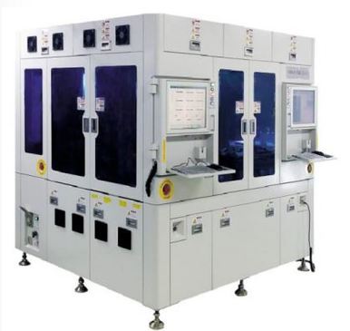
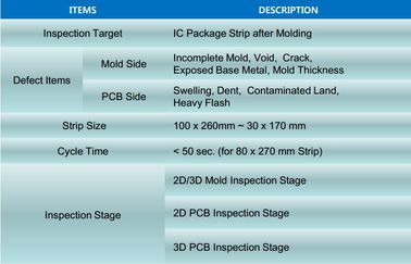
This is a type of equipment designed for inspecting defects that may occur at the upper and lower surfaces of package strips rolled out from the molding process which is one of semiconductor package production processes. Unmolded areas, cracks, exposed base metals, or the like are inspected by the 2D inspection on upper mold surfaces, and land contamination, the swellings and dents of PCB surfaces are quantitatively inspected by the 2D/3D inspection on lower PCB surface. *Highlights -Overcoming the limitations of conventional 2D inspection by using 3D measurement method -Various defects on mold surface and PCB surface are detected -Quick and easy programming using the registered templates -The index information of defective packages are obtained along with the positions whtere the defects occurred -All measurements and inspection results are stored in the database -Calculation and evaluation of process capability indices -Defect review functions (defect images, measured defect data, inspection results) |
|
|
Stacked Package Inspection System |
|
*Description
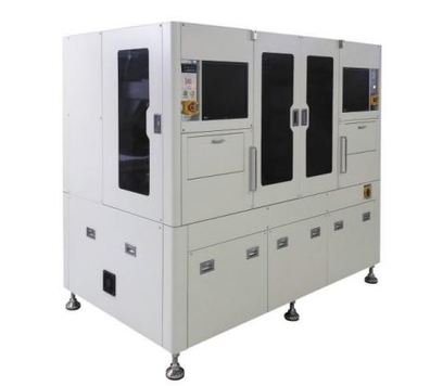
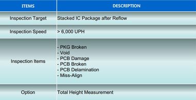
This is a type of equipment designed for measurements(Total Height, Gap, Misalign) of package which is loaded on Boat after Stacking & Reflow Process, and designed for inspecting defects that may occur the surfaces of package(4 Sides) in the Package Assembly Process. Inspection items are PKG broken, Woid, Misalign, PCB damage, PCB broken, PCB delamination, and Metal exposure. *Highlights -High-precision inspection on a scale of a few㎛ -Vision Inspection for the 4 sides and Good/NG sorting -The Unit Map information on Boat are supplied -High throughput resulting from ultra-high speed processing -All measurements and inspection results are stored in the database -Defect review functions (Defect images, Measured defect data, Inspection results) |
CMOS Image Sensor Inspection System |
|
*Description
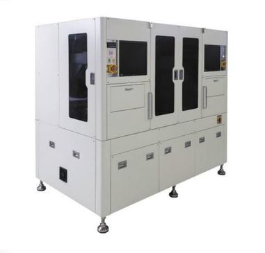
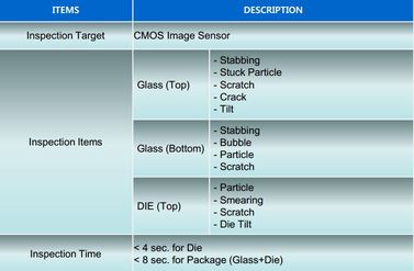
This is a type of equipment designed for inspecting defects that may occur the pixel area of Sensor Die Surface(Top) after Die-Bonding with the state of PCB Strip and the package surface of Cover Glass(Top, Bottom) & Die(Top) that are stacked by unit on Tray in the CIS Package Assembly Process. *Highlights -High-precision inspection for diminutive defect on a scale of the Image Sensor Pixel Size -High-precision auto-inspection in layer using auto-focusing function -The index information of defective packages are obtained along with the positions where the defects occurred -High throughput resulting from ultra-high speed processing -All measurements and inspection results are stored in the database -Defect review functions (defect images, measured defect data, inspection results) |
Wafer Defect Inspection System |
|
*Description
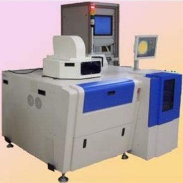
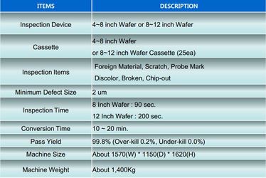
This is an automatic inspection system comprehensively inspecting the foreign material, broken, chip-out, scratch, PAD Mark, discolor defects on the surface of Wafer CMOS CELL. *Highlights -High Precision Alignment -Wafer Reading Functions -Wafer Cell Editing Functions -Automatic Z-axis Compensation(Auto-Focusing) -High Reliable Defect Detection&High Accurate Measurement -Wafer Tracking Functions -Defect Review Functions -Defect Cell Map -SPC Functions -User-friendly Man-machine Interface |

Partner

