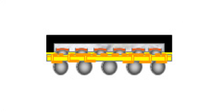
*Overview -A CSP substrate utilizing conductive solder bumps for electrical connection between die and substrate -Suitable for faster data transmission by using flip chip bonding *Feature -Array type lead free solder bump and stack ball -Build - up technology plating available -Stack via available -MLCC embedding
Thin CSP
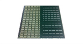
*Overview -Multi Chip Packages require thinner substrates to stack more chips in a single package. *Feature -80~100um total thickness using 35~40um laminates - For proper handling of thin substrates, special guide can be applied -Flat surface -Via available (Cu filled)
Build - up CSP
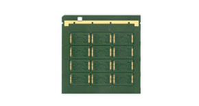
*Overview -High Functionality High Density packages using HDI build - up lamination -We use standard materials and laser drilling to create leading technology, multi-layer, high density package substrates. *Feature -High density build-up structure -Via fill plating available -Stack via available
BOC
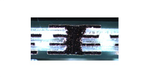
*Overiew -Fine Line Technology enables high speed DDR DRAM to reduce signal noise by using a short electrical path *Feature - Slot Fabrication by Router of Punching without additional shaving -Fine Line Technology(L/S=25㎛/25㎛)by subtractive process or MSAP process -Dual substrates process available -Multi Layer Process available